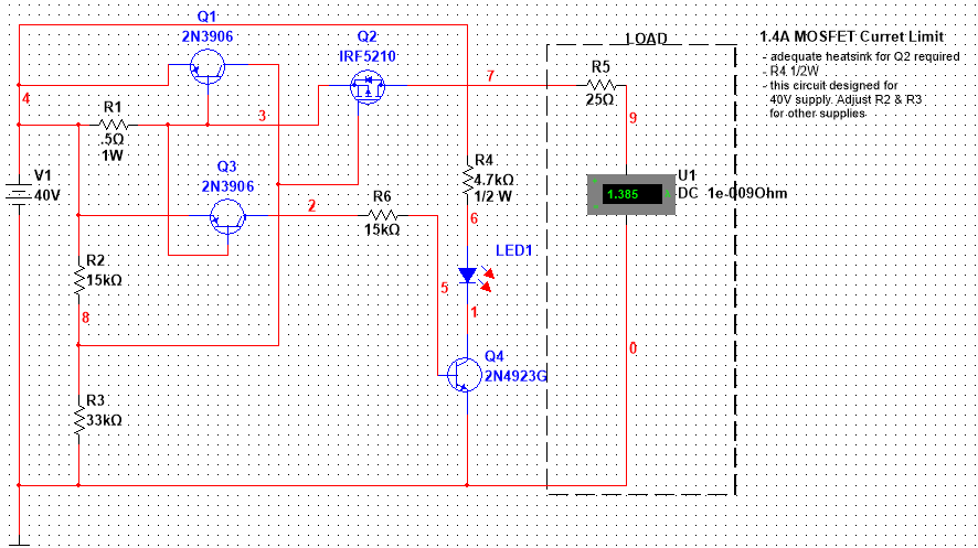
This circuit provides a current-limited DC output voltage. As shown, the
circuit limits the output current to a maximum of 1.4 A and includes a visual
indicator of a current-limit condition. During normal operation (i.e., load
current is less than the limit value) the MOSFET should be fully on. As the
load increases (load resistance decreases) to the point at which the current
limit is reached, the circuit should decrease the output voltage to ensure the output current
design limit is not exceeded.
Design Details -- How it Works
Referring to the schematic, R2 and R3 form a voltage divider providing bias
to Q2. The supply voltage for this circuit is 40V. From the
datasheet for the IRF5210, the minimum gate
to source voltage is $V_{GS} = -20V$. Since the gate voltage is supplied from the divider
network, we have:
\[\frac{40R_3}{(R_2+R_3)} - 40 > -20 \]
Simplifying:
\[\frac{40R_3}{(R_2+R_3)} > 20 \text{ or } 40R_3 > 20(R_2+R_3)\] Therefore, $$20R_3 > 20R_2 \text{ or }
R_2 <
R_3$$ However, to turn Q2 on, we must ensure that the gate voltage is less
than the gate threshold voltage $V_T$. Moreover, since we
want Q2 fully on, we should design for a gate to source voltage $<-10V$. Note that this value
can be obtained from the datasheet.
Therefore,
$$\frac{40R_3}{(R_2+R_3)} -40 < -10 \text{ or } 10R_3 < 30R_2$$ Rearranging yields:$$R_2 > \frac{1}{3}R_3$$
This yields the following range for R2:
$$\frac{1}{R_3} < R_2 < R_3$$ Selecting $R_3=33k\Omega$ implies$$11k\Omega < R_2 < 33k\Omega$$.
Given this, a value of $R_2=15k\Omega$ was selected.
These values for $R_2$ and $R_3$ yield a bias voltage of 27.5V or $$V_{GS} = 27.5 - 40 = -12.5V$$
which is well below the fully-on voltage of -10V and well above the minimum gate to source voltage of -20V.
The current limiting capabilities of the circuit are provided by sense
resistor $R_1$ in conjunction with the 2N3906
PNP transistor, Q1 . A voltage drop will develop across sense resistor, $R_1$, as
current, $I_L$, passes from the positive supply voltage through Q2 to the load. This voltage drop is given by Ohm's law as
$I_LR_1$ and appears across the $V_{EB}$ junction of Q1.
Transistor, Q1, will remain off until its emitter to base voltage exceeds the
emitter to base forward diode drop (approximately .7V). Therefore, from
Ohm's law, the value of the current through $R_1$ at which Q1's emitter to base
voltage exceeds the .7V diode drop is given by: $.7V = .5I_L$ or $I_L=1.4A$.
How does this limit current, $I_L$? As $V_{EB}$ increases above
.7V, current begins to flow out of the collector of Q1 and through $R_3$ to ground.
Therefore, the total current passing through $R_3$ increases
by the amount supplied by the collector of
Q1. The net effect of increased current through $R_3$ is (again, by Ohms Law) an increase in the gate
voltage of Q2, and therefore an increase in the $V_{GS}$
voltage. $V_{GS}$ will continue to rise until it approaches $V_T$
at which point Q2 will begin to shutdown, reducing the load current $I_L$, and hence the collector
current of Q1; thereby, reducing the $V_{GS}$ voltage.
Ultimately, a balance will be reached whereby Q2 supplies sufficient current to
supply a $V_{GS}$ value that limits $I_L$ to approximately 1.4A.
Transistors Q3 and
Q4 in conjunction with
LED D2 and limiting resistor R5 form the current limit indicator sub
circuit. The behavior of the current limit indicator sub circuit is similar to
the current limit circuit described above in that the collector of Q3 provides
current to the base of Q4 in response to an increase in the $V_{EB}$
voltage of Q3 as the current through sense resistor R1 increases.
Note that a 2N4923 transistor was chosen for Q4 rather than a 2N3904 because of the collector to emitter voltage.
Output Current Versus Load
The graph below plots the current through a resistive load (the green trace), the source-to-drain voltage (the light-blue trace), and the gate-to-source voltage
(the dark-blue trace) as the load resistance varies.
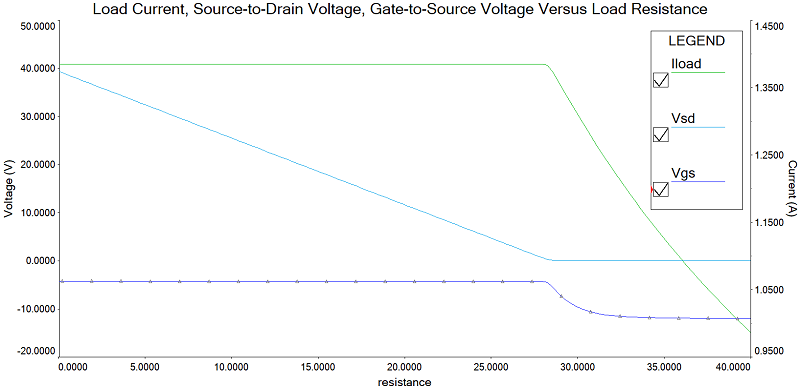
From the graph, the gate-to-source voltage is below the turn-on voltage with a high-resistance load. (i.e., the MOSFET is fully on)
As the load resistance is decreased (moving left on the graph), the current through the load
begins to increase, and the gate voltage begins to increase until the gate-to-source voltage is reduced
to the point where the load current is limited to approximately 1.4A as the resistive load continues to decrease.
Further decrease in the load resistance forces the source-to-drain voltage to increase, preserving the 1.4A current through the load.